(2013/11/27)

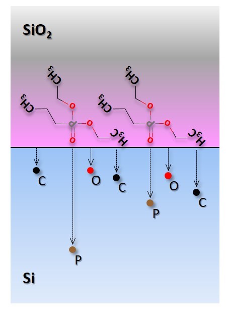
The fabrication of future nanoscale semiconductor devices calls for precise placement of dopant atoms into their crystal lattice. Monolayer doping combined with a conventional spike annealing method provides a bottom-up approach potentially viable for large scale production. While the diffusion of the dopant was demonstrated at the start of the method, more sophisticated techniques are required in order to understand the diffusion, at the near surface, of P and contaminants such as C and O carried by the precursor, not readily accessible to direct time-of-flight secondary ion mass spectrometry measurements. By employing atom probe tomography, we report on the behavior of dopant and contaminants introduced by the molecular monolayer doping method into the first nanometers. The unwanted diffusion of C and O-related molecules is revealed and it is shown that for C and O it is limited to the first monolayers, where Si–C bonding formation is also observed, irrespective of the spike annealing temperature. From the perspective of large scale employment, our results suggest the benefits of adding a further process to the monolayer doping combined with spike annealing method, which consists of removing a sacrificial Si layer to eliminate contaminants.
Nanoscale, Vol. 6, 706 (2014).
http://dx.doi.org/10.1039/C3NR03605G


